PCB Business Cards
I have always been fascinated with PCB business cards. From the moment I found out about them, what appealed to me the most was always how much intricacy and thought can go into each design. Whereas traditional business cards pose a challenge in graphic design, that is pretty much the extent of their complexity.
PCB Business cards, on the other hand, have the potential to integrate working circuitry and mechanisms to perform basic functions. When coupled with the size constraint of the standard business card, this creates a unique challenge to tackle. As a result, the cards that are designed are, in my opinion, much cooler than traditional business cards that serve no other purpose than providing information.
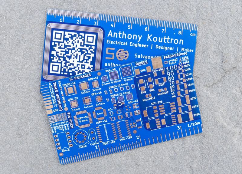
Anthony Kouttron’s card. This one is focused heavily on acting as a reference card for electrical engineers, integrating as many footprints into its design as possible. His design also features a functional NFC reader, if the chip is soldered on.
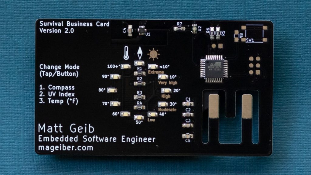
Another example coming from Matt Geib. What I find fascinating about this card is the integrated button cell slot. Utilizing the natural flex of the FR4, one can securely slot a button cell into it to power an array of LEDs.
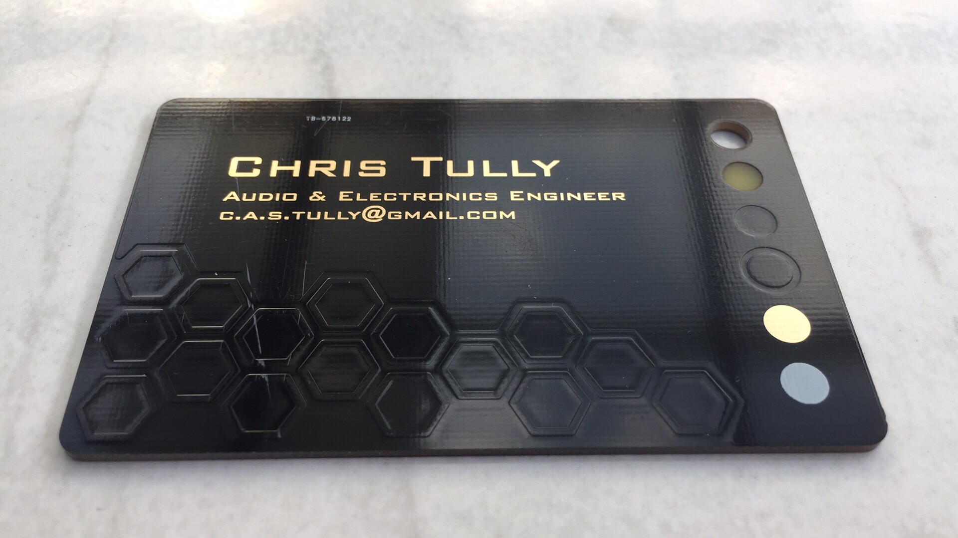
Yet another example from Chris Tully. Visually, I find this one the most interesting, due to how he utilized the copper under the soldermask. By using copper fills with some negative space, he was able to create the hexagon texture under the soldermask, even without exposing any copper.
Initial Challenges
These are just a few examples of the cards I found searching Google, but overall I would say these 3 were the most influential for my design. Initially, I wanted to pursue a direction similar to Matt Geib’s example, where the card has some sort of built-in electronic function. Integrating NFC, LEDs or even tiny speakers were all possibilities I looked into for my design.
However, the biggest common problem I found between all these is that none of these functions can work without some sort of componentry / chips soldered to the surface of the card. This sort of ruined it for me, as soldered chips would add a significant amount of thickness and roughness to the card, making it impractical to carry in a wallet. To me, this kind of defeats the purpose of the business card in itself, as it is meant to be easily carried and shared.
I spent a lot of time brainstorming what kinds of things a PCB business card can do, but unfortunately there were very few options available that do not require surface mounted componentry. I felt sort of stuck. I knew I wanted my card to have some sort of function beyond simply providing information, yet every option seemed impractical to integrate.
Because of this roadblock, I ended needing to take a step back from the project for a little while. It wasn’t until a few months later when it hit me: I had been so focused on the electrical capabilities of the pcb, that I had completely overlooked another huge area of exploration, the physical capabilities of FR4 as opposed to traditional paper.

Chicken scratch of when I first got the idea, late at night, drawn on my iPad notes app
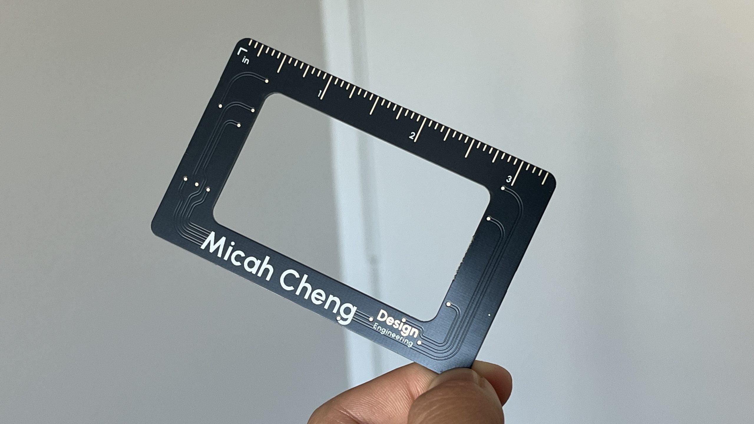
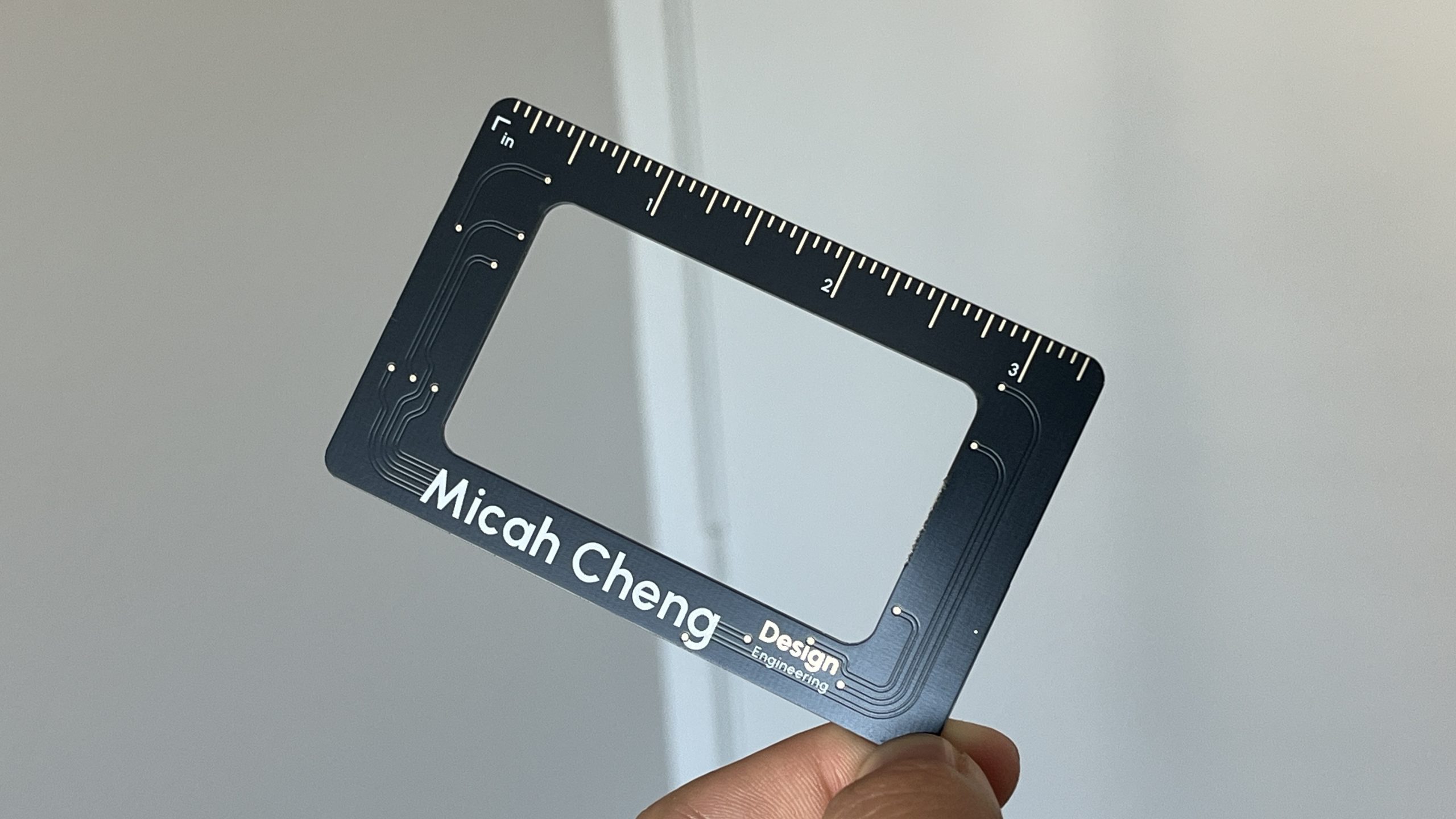
That’s when I got the idea: a “frame” of a business card, keeping the same outer footprint of a standard card, but with a hollow center that allows you to see through the middle of the card.
Concept Development
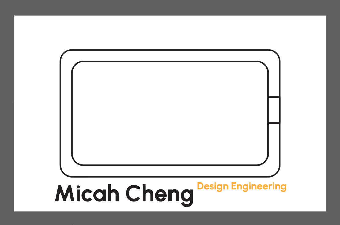
Originally, I thought it would be a good idea to mock up my design in Illustrator, but I soon realized it is much more efficient to simply make it in KiCad from the beginning.
I ended up going with JLCPCB as my PCB manufacturer, as they are inexpensive and I have had good experiences with them in the past.

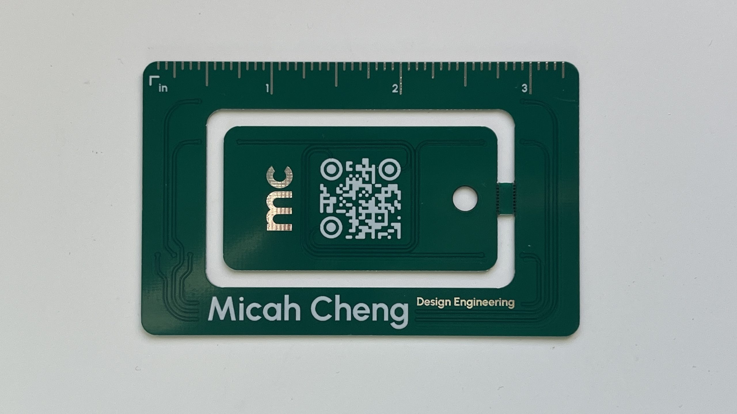
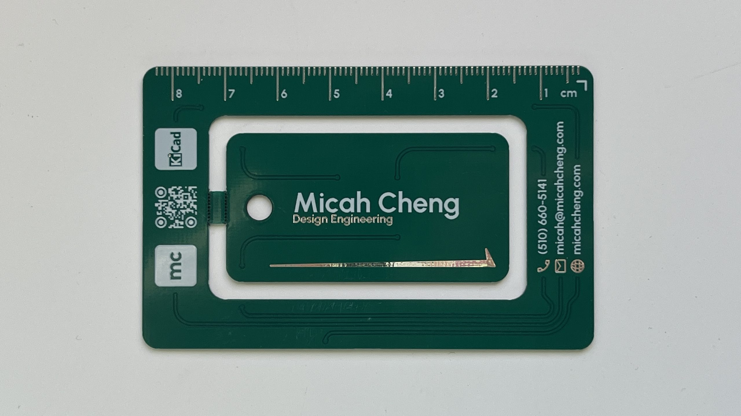
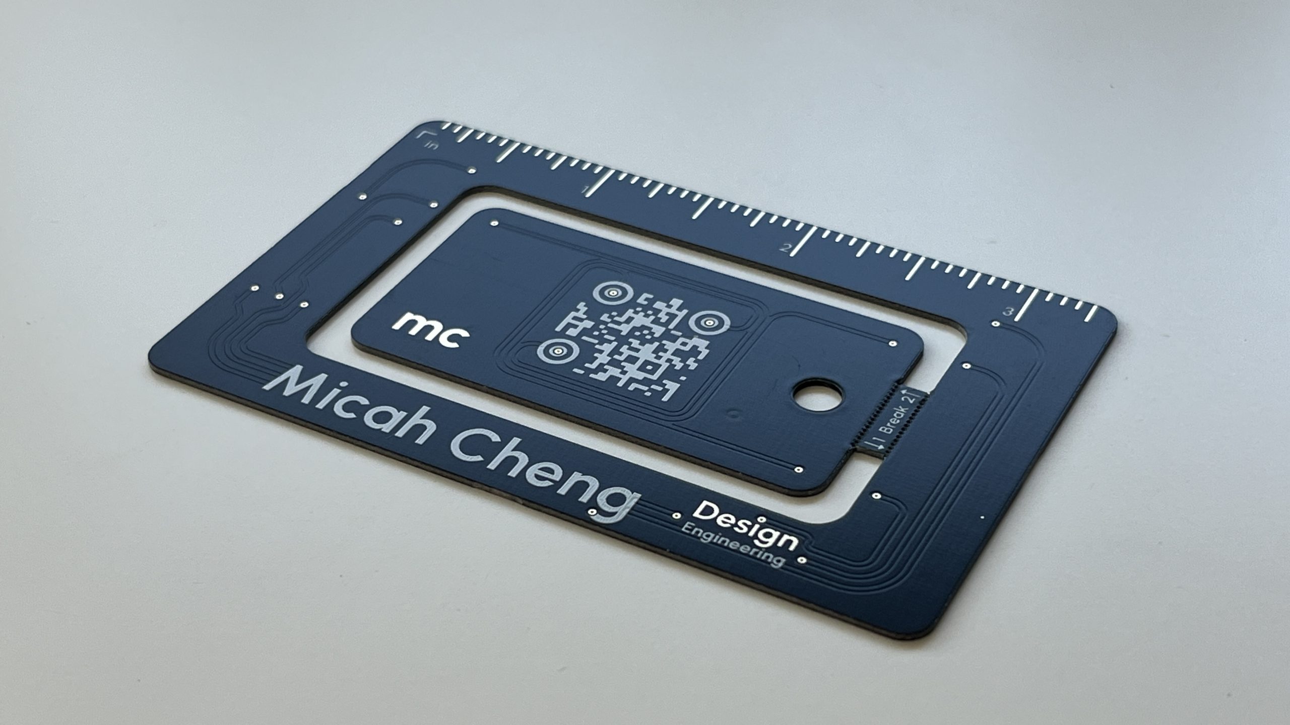
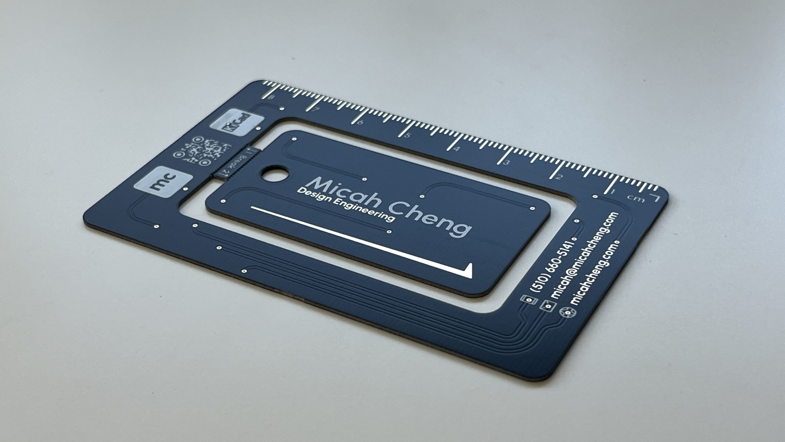
This is the first iteration of the design. I opted not to add any functional electrical circuits, as I wanted to keep the slim profile of the PCB without adding the unnecessary thickness of componentry. The only practical feature I added to the card was simply the Imperial/Metric ruler along the top edge of the card. I think I might actually find this useful in the future, as I often use Metric units in my design, and by having this handy ruler in my pocket at all times, I can quickly get a frame of reference for what size things might be.
Additionally, I experimented with adding in some traces, to make it look as if the printed details, such as my name or contact information, could look somewhat like components all wired together.
Another challenge I faced was adding meaning to the large hole in the middle of the card. I knew I wanted the outer part of the card to have a large hole in the middle, but bringing purpose to that hole was another story.
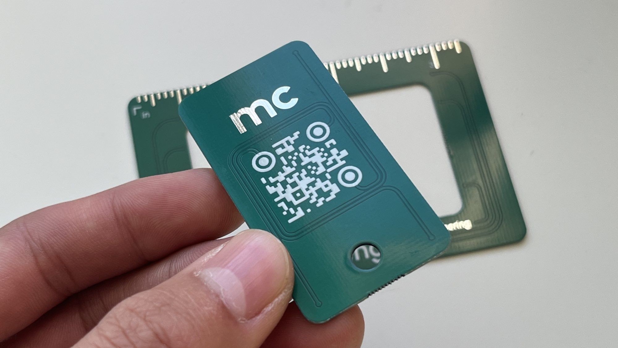
The solution I ended up coming up with was to create a removable keychain module in the center of the card. Using breakaway tabs, I make a neat little keychain that snaps out of the main body.
Room for Improvements
While my first design was functional, I was far from satisfied with it. With the next iteration, I made several improvements.
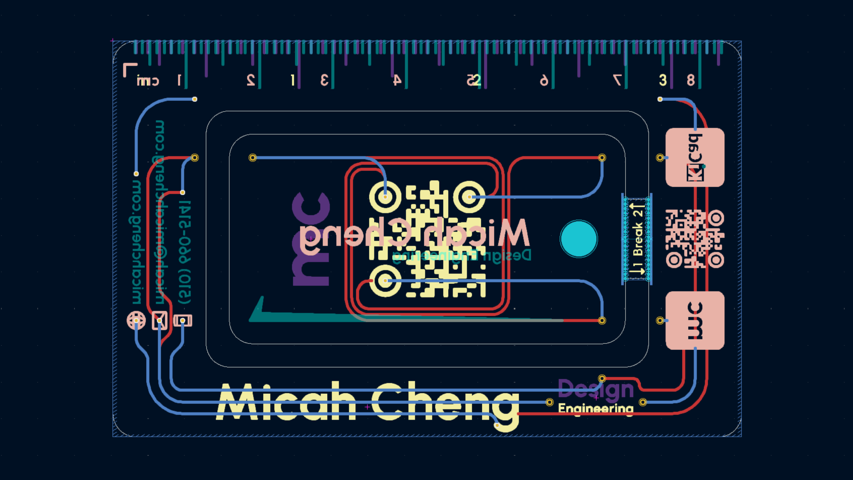
Improved Traces & added Vias
First and foremost, I greatly improved the routing of the traces. On the previous iteration, the traces stopped next to the “components,” but on this version, I made the traces directly touch the them as they would on an actual PCB.
Additionally, after discussing the design with one of my professors, he suggested to me to add actual Vias and Plated Through Holes (PTHs), as it would further show off the fact that the top and bottom set of traces, are in fact, connected to each other.
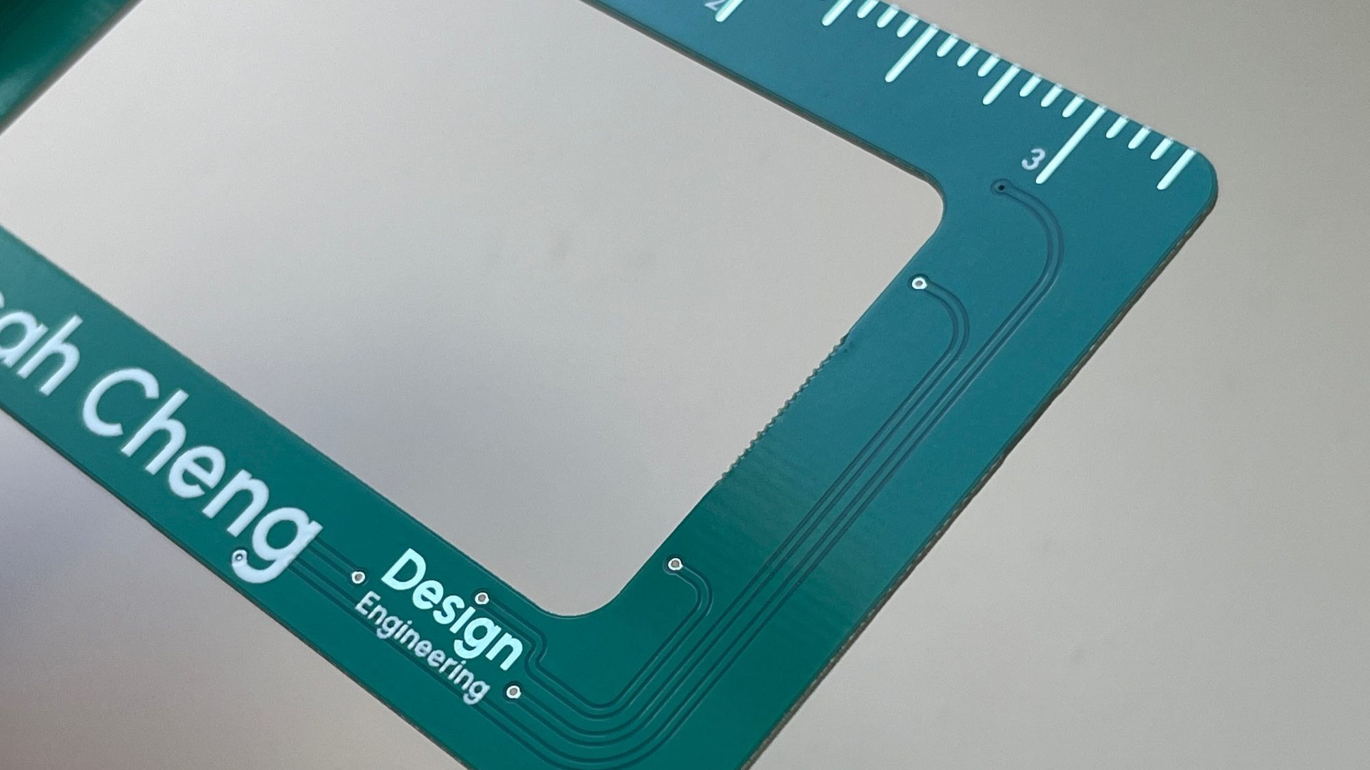
Some Plated Through Holes, and a Via on the top right.
Improved Break Tab
Next, I modified the break tab that connects the keychain module to the outer frame of the card. The original design was weaker than I wanted it, so I made the tab a little wider. I also found that it was easier if you break the outer edge before the inner, so I added a little graphic that tells which edge to break first.
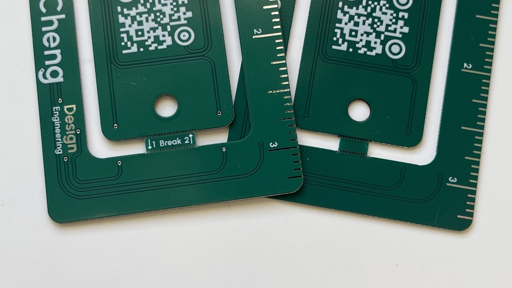
Right card: First iteration
Left card: Second iteration – Note the improved break tab.
Final? Iteration
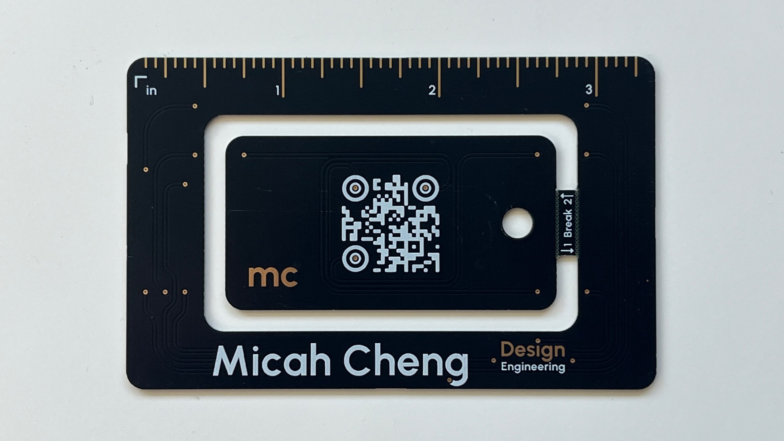
After getting my hands on the second iteration, there were just a few more changes I wanted to make, Because, at this point, I was pretty confident in how refined my design was, I went ahead and splurged on the Black soldermask + ENIG combo, giving me a gorgeous black and gold finish. This finish costs significantly more than the green + Leadfree HASL I had been using previously, which is why I did not opt for it earlier.
Changed all Vias to PTHs

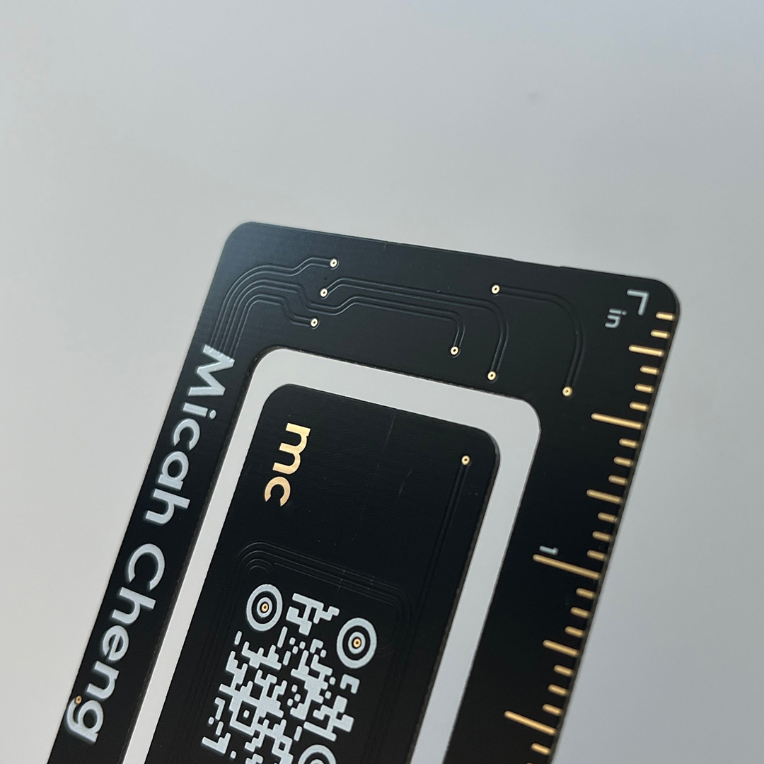
With this iteration, I decided to change all Vias to PTHs, because I decided they look much better. Especially when using the ENIG finish on the black silkscreen, it really makes the features pop out.
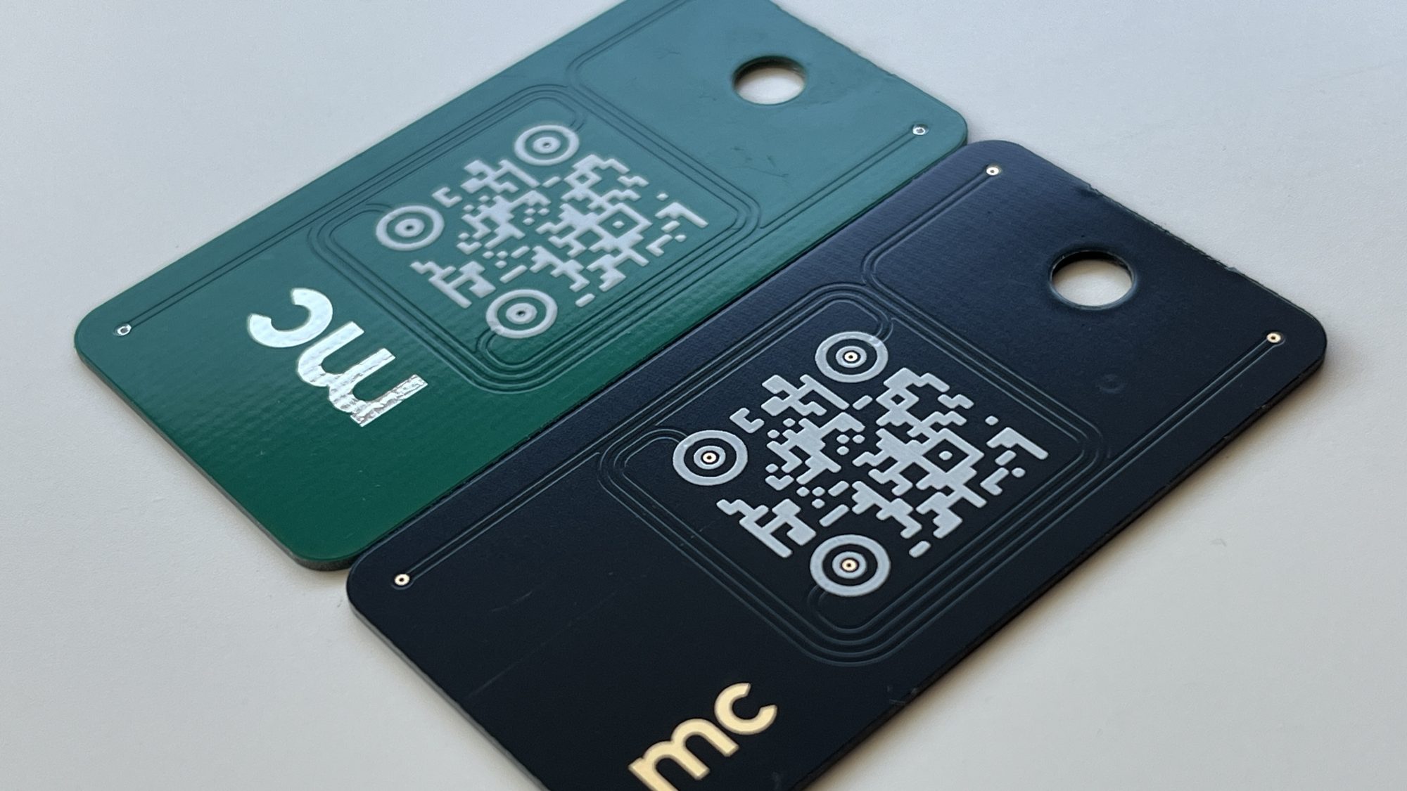
Even for the keychain module, I think the PTHs look much better than the Vias. Notice the difference inside the homing circles of the QR code.
Differences between LeadFree HASL and ENIG Finish
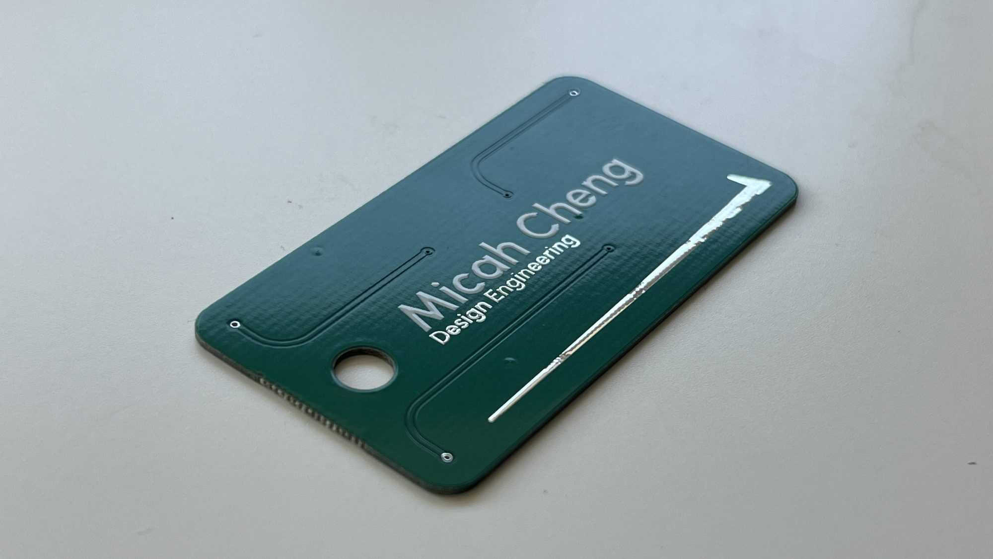
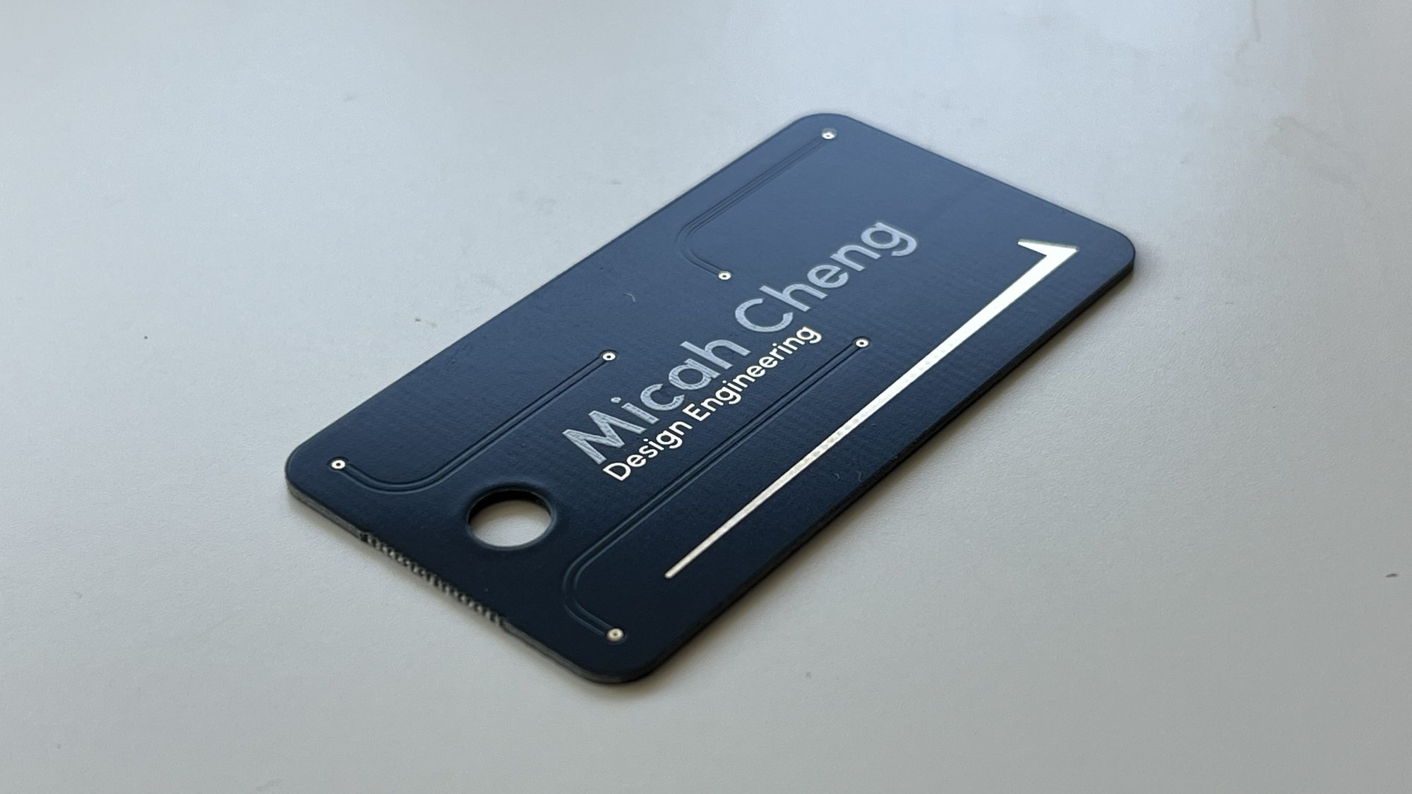
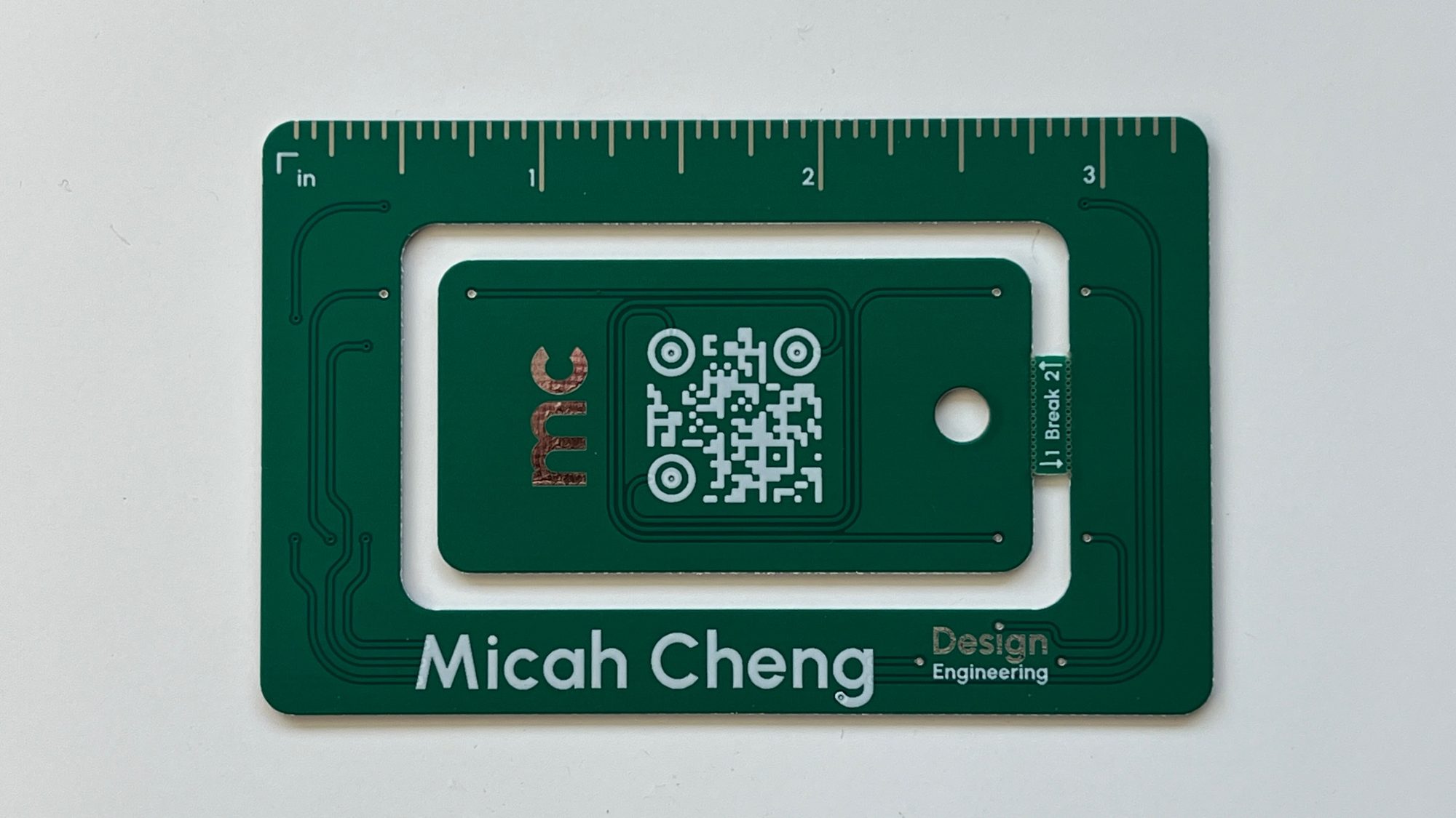
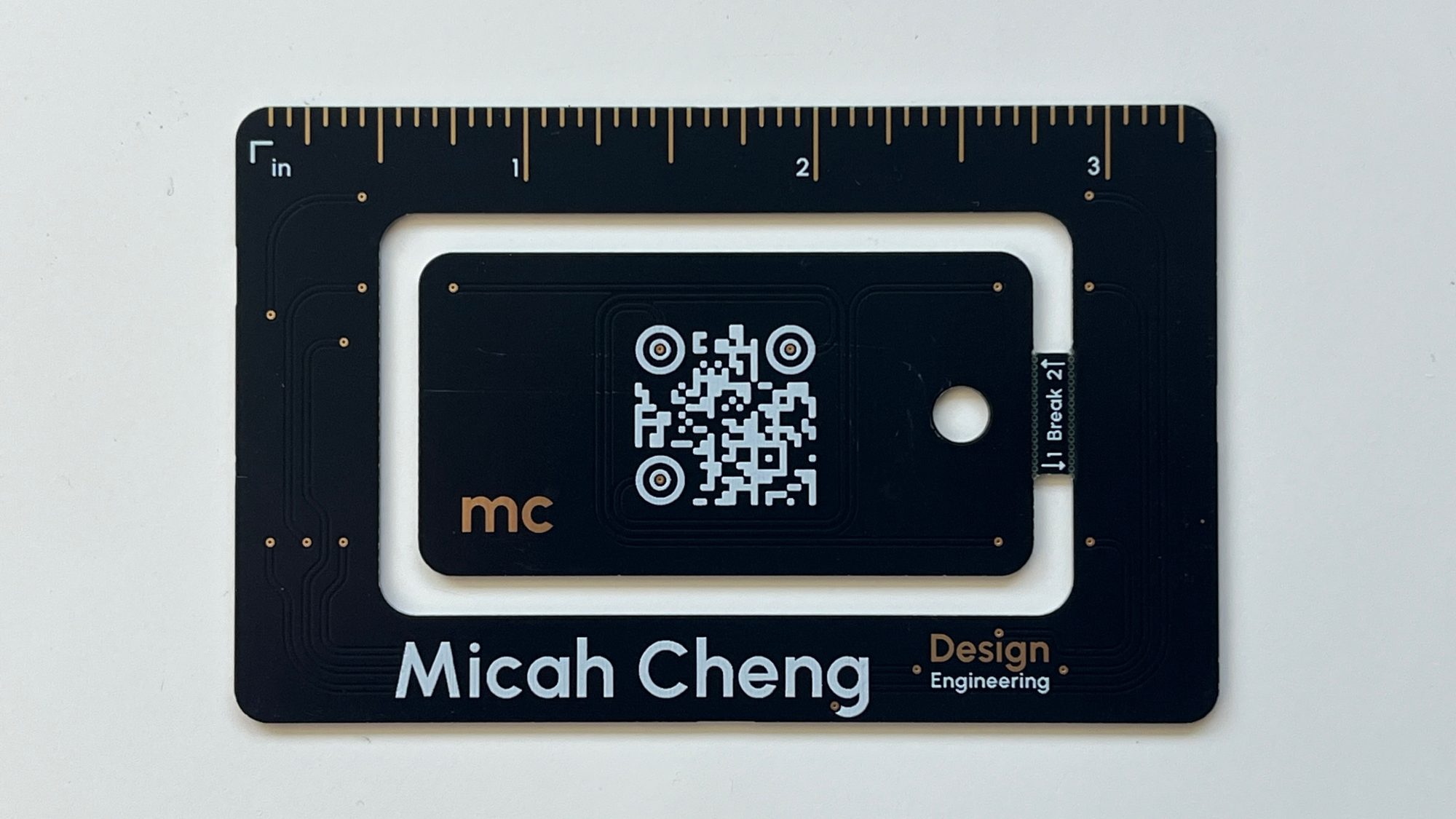
Not only, in my opinion, is the gold color of the ENIG finish prettier than HASL, it turned out much crisper than the previous version. This could possibly be just a JLCPCB quirk, but the ENIG finish came out visually perfect, whereas many of the HASL finish versions came out a little bit lumpy or wobbly.
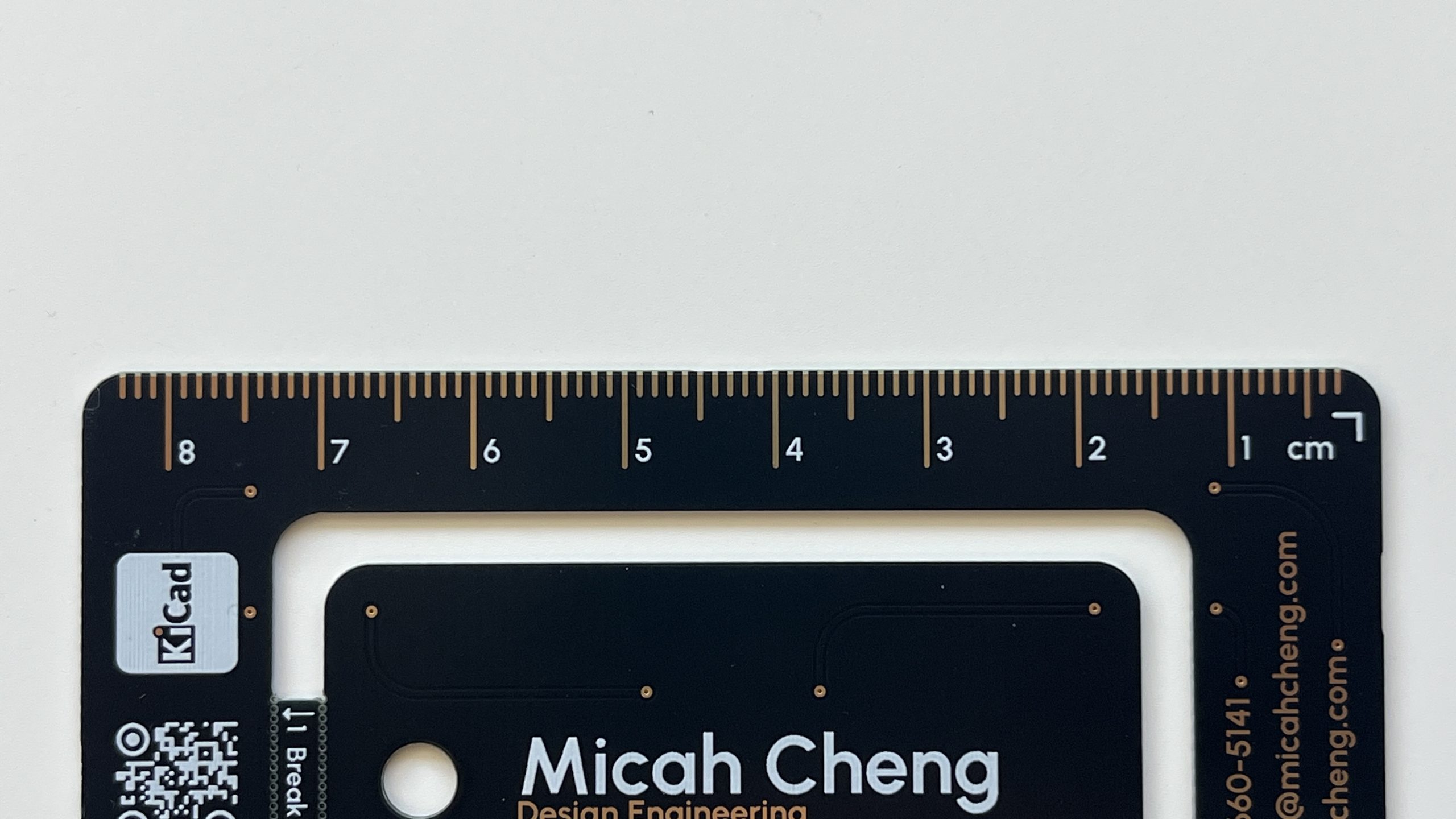
Even the ruler turned out perfect.
Closing Thoughts
Originally, I had intended to create a run of white business cards after this, as for some reason, the white soldermask version cost even a little bit more than the black. However, after seeing the black soldermask with ENIG finish in person, I was so pleased with how it turned out that I decided to simply keep the color for now. In the future, I may further explore color options, but for now, I am satisfied with how these are.
If you are interested in getting your hands on one of these, don’t hesitate to reach out to me, and I’d love you connect with you!
Without further ado, here’s a gallery of the final product:
